RISC-V CPU
Overview
This project spans the full design stack of a full-custom CMOS RISC-V CPU, completed across ECE 425. The work begins from individual standard cells designed and verified in Cadence Virtuoso, built up into a bitsliced 32-bit datapath, and culminates in a complete CPU with a synthesized control unit integrated back into Virtuoso for a final full-chip layout.
Each cell and component was drawn at the transistor level, verified with DRC and LVS, and assembled hierarchically. The control unit was synthesized using Synopsys Design Compiler and placed-and-routed with Cadence Innovus before being stitched back into the Virtuoso environment alongside the hand-crafted datapath.
Standard Cell Library
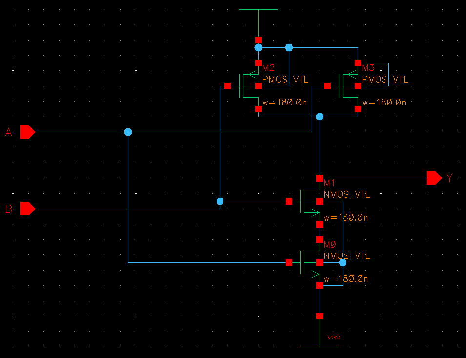
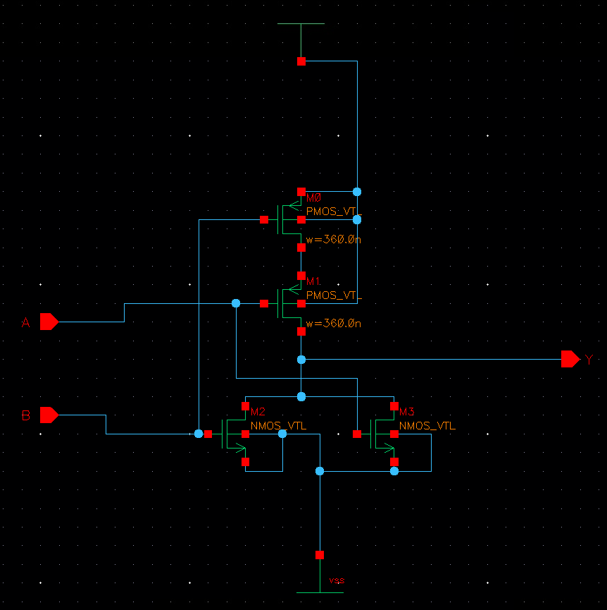
A full-custom CMOS standard cell library of 13 cells was designed from scratch in Cadence Virtuoso. Every cell passed DRC and LVS verification. Heights are fixed to a shared rail pitch; widths vary by logic complexity.
| Cell | Expression | Width (µm) |
|---|---|---|
| and2 | Y = A & B | 0.8225 |
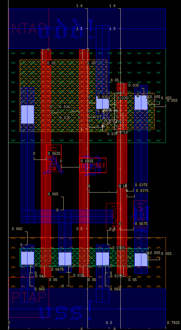
| aoi21 | Y = ~((A & B) | C) | 0.76 |
| buf | Y = A | 0.6125 |
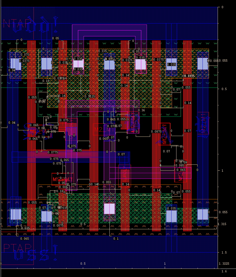
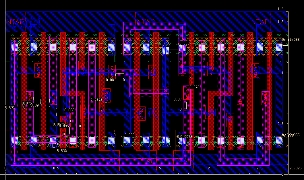
| dff | d-flip-flop | 2.7825 |
| latch | d-latch | 1.67 |
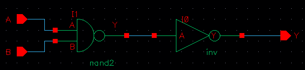
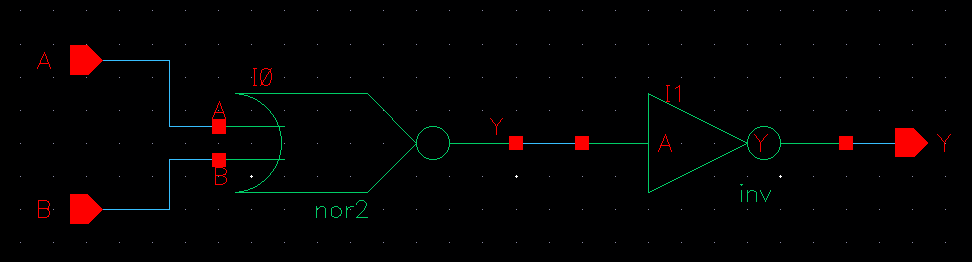
| inv | Y = ~A | 0.3725 |
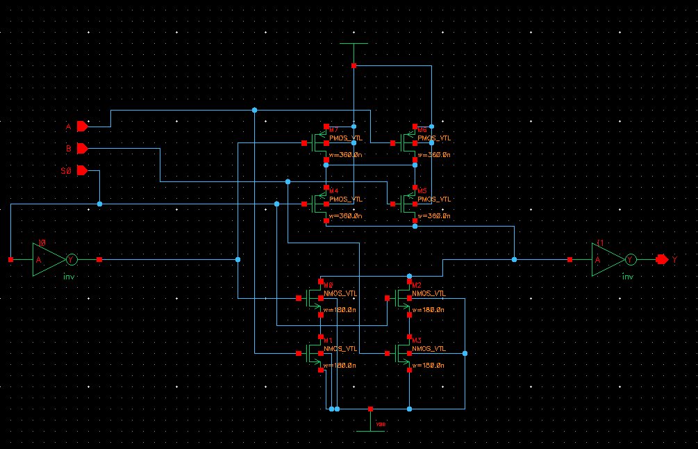
| mux2 | Y = (~S0 & A) | (S0 & B) | 1.3225 |
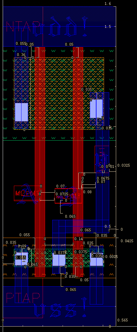
| nand2 | Y = ~(A & B) | 0.565 |
| nor2 | Y = ~(A | B) | 0.5665 |
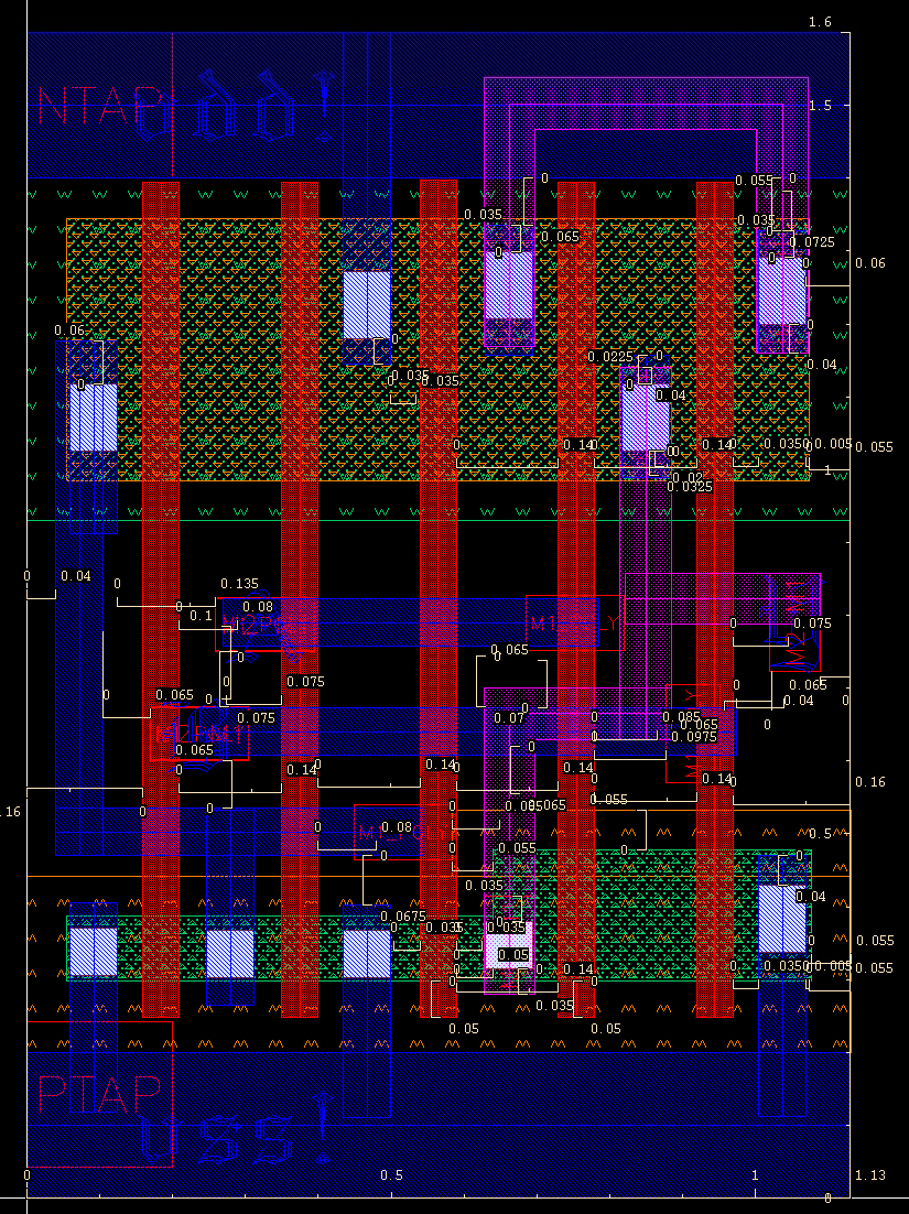
| oai21 | Y = ~((A | B) & C) | 0.76 |
| or2 | Y = A | B | 0.785 |
| xnor2 | Y = ~(A ^ B) | 1.145 |
| xor2 | Y = A ^ B | 1.1325 |
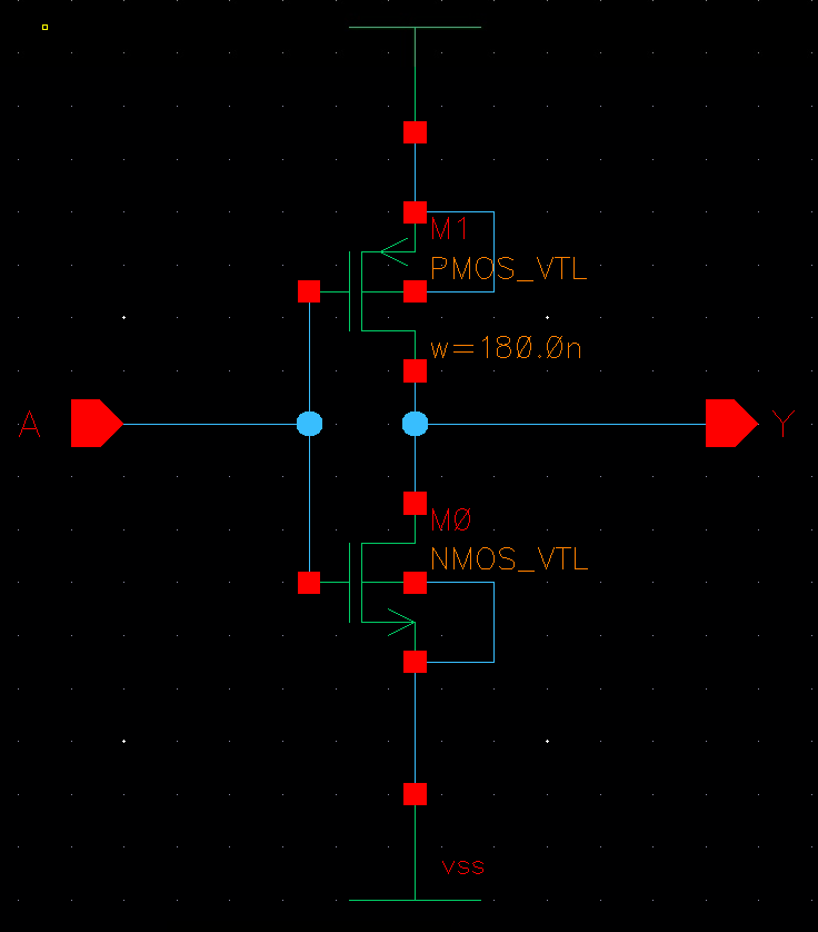
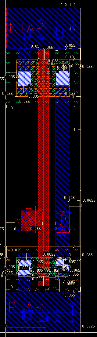
A PMOS pull-up and NMOS pull-down form the complementary network for logical inversion. As the smallest cell in the library, it serves as the building block for the buffer and several compound gates.

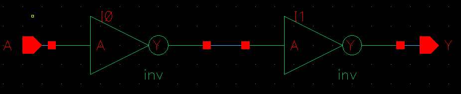
Two cascaded inverters restore signal strength without changing logic value. The second stage is sized larger to drive heavier fanout loads.
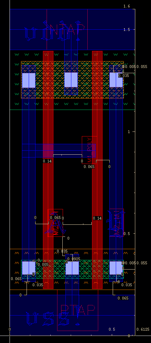
Series NMOS pull-down and parallel PMOS pull-up implement the universal NAND function. One of the most area-efficient gates in the library.
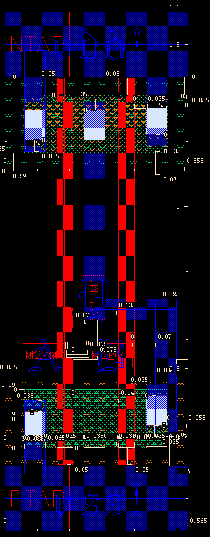

Parallel NMOS pull-down and series PMOS pull-up realize the NOR function. The stacked PMOS network requires wider transistors to match drive strength.

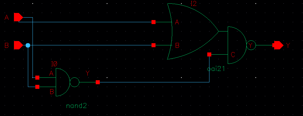
Implemented as a NAND gate followed by an inverter stage. DRC and LVS both verified clean.
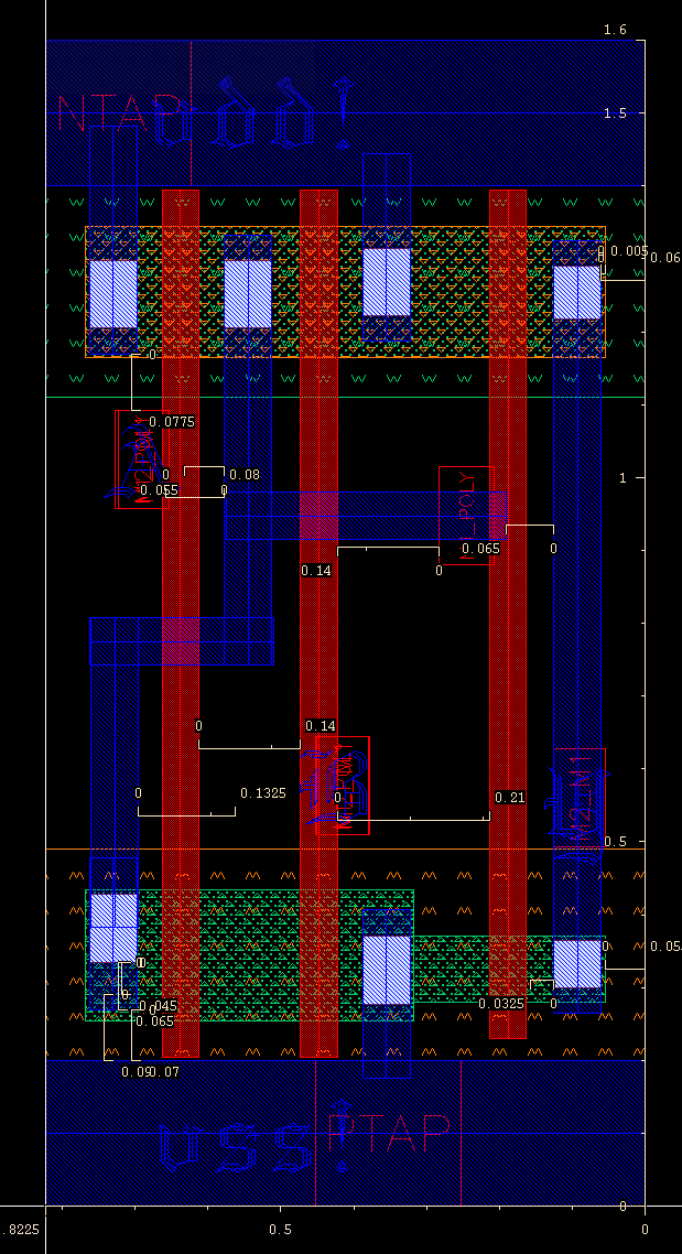
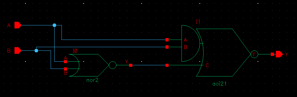
Implemented as a NOR followed by inversion. The pull-down network uses parallel NMOS and the pull-up uses series PMOS.
Exclusive-OR realized using a transmission-gate based topology, balancing performance and area. Used extensively in the ALU sum path.
Complement of XOR; outputs high when both inputs match. Used in the comparator path of the bitslice to detect equality.
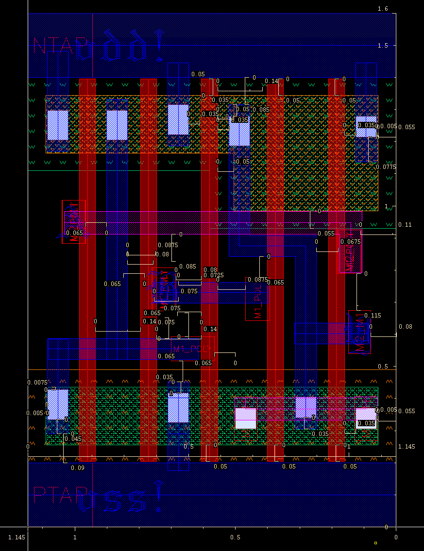
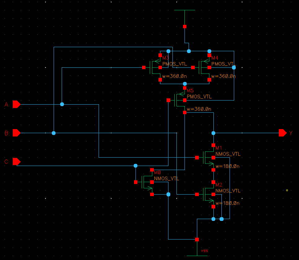
Compound cell implementing AND-OR-Invert logic in a single CMOS stage, reducing transistor count and propagation delay compared to a gate-by-gate implementation.
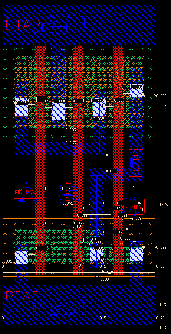

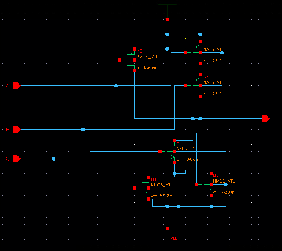
Dual of the AOI21 cell. Combines OR-AND-Invert in one complementary CMOS network, useful in carry-lookahead and priority logic paths.
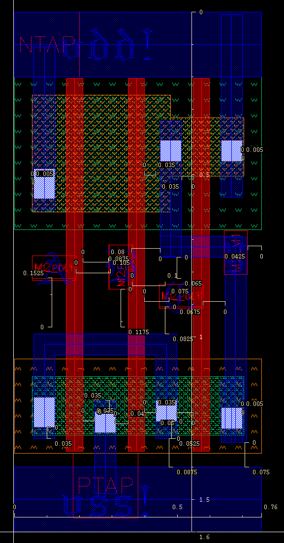

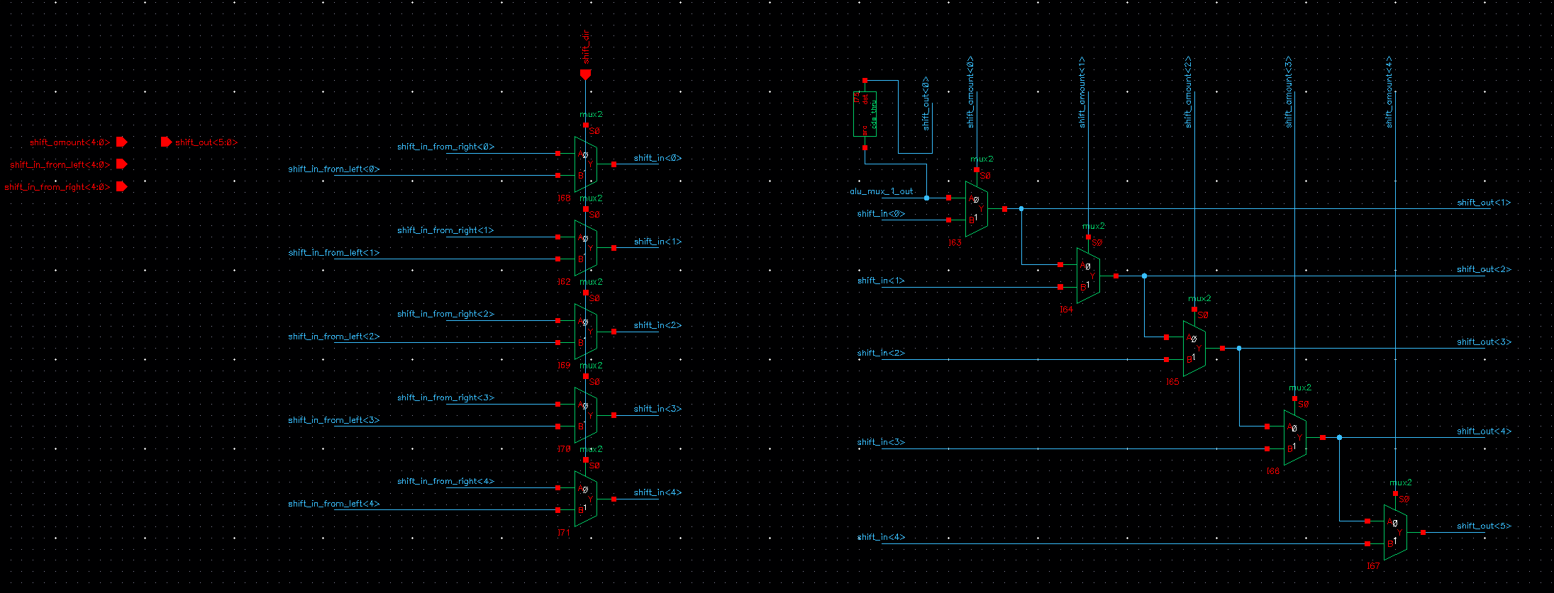
Transmission-gate based 2:1 mux selects between inputs A and B using select signal S. Critical for the ALU operand select and barrel shifter steering logic.

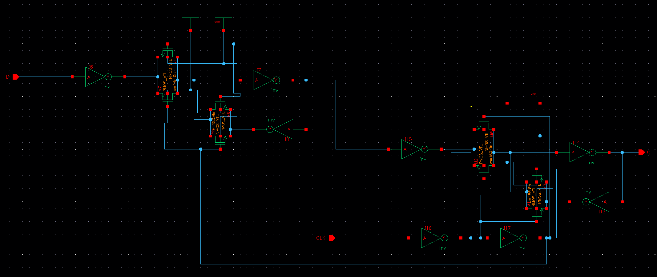
Level-sensitive latch is transparent when EN is high and holds state when EN is low. Forms the master stage of the edge-triggered flip-flop.
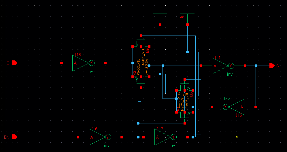
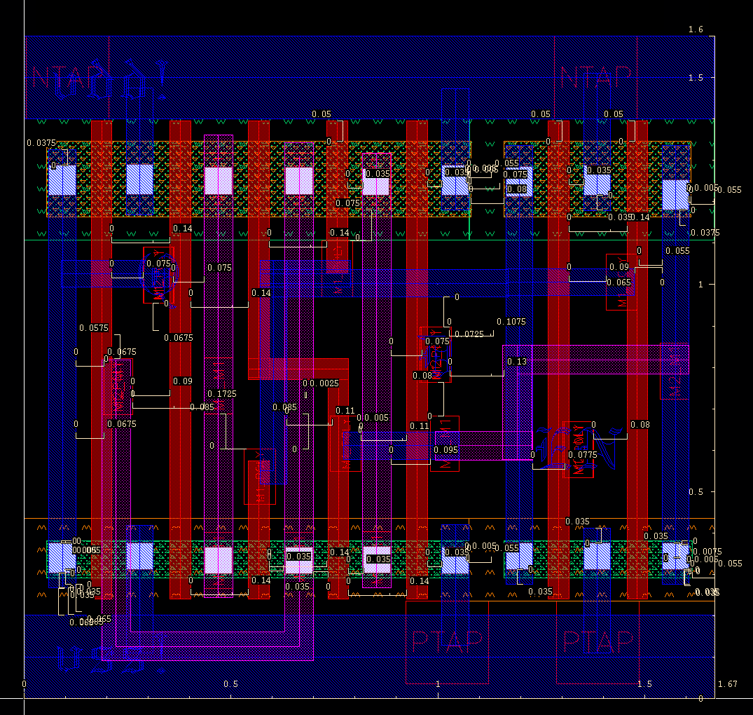

Positive-edge-triggered flip-flop built from two cascaded latches. The largest cell in the library; used for the program counter, register file bits, and pipeline registers.

RISC-V CPU Datapath
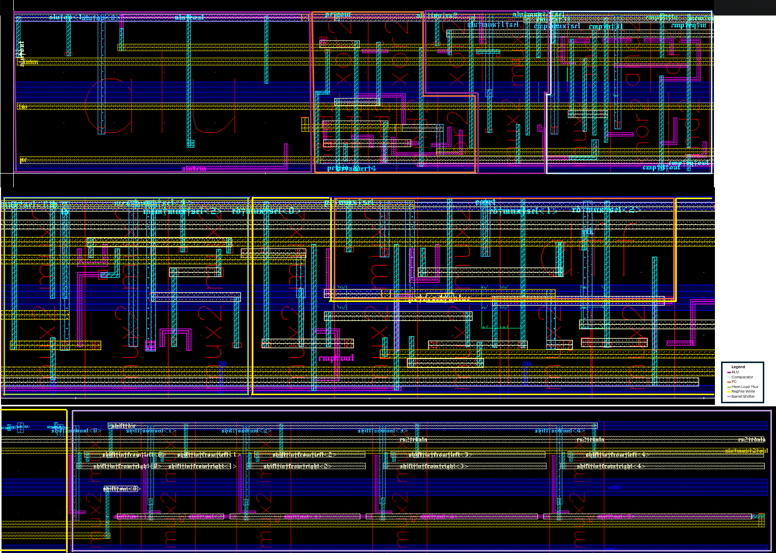
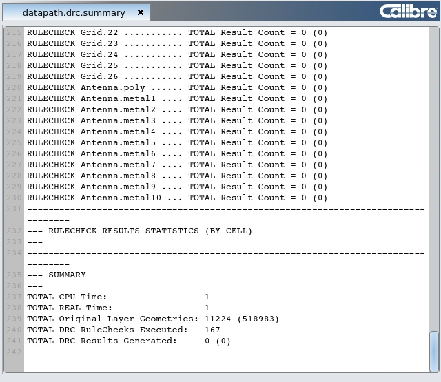
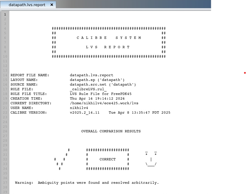
The standard cell library is the foundation of a full-custom 32-bit RISC-V datapath designed using a bitslice methodology. Each bitslice column implements one bit of all datapath operations — ALU arithmetic, shift, compare, register read/write — and is tiled 32 times to form the full-width datapath. The design passed DRC and LVS at the top level.
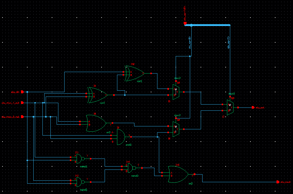
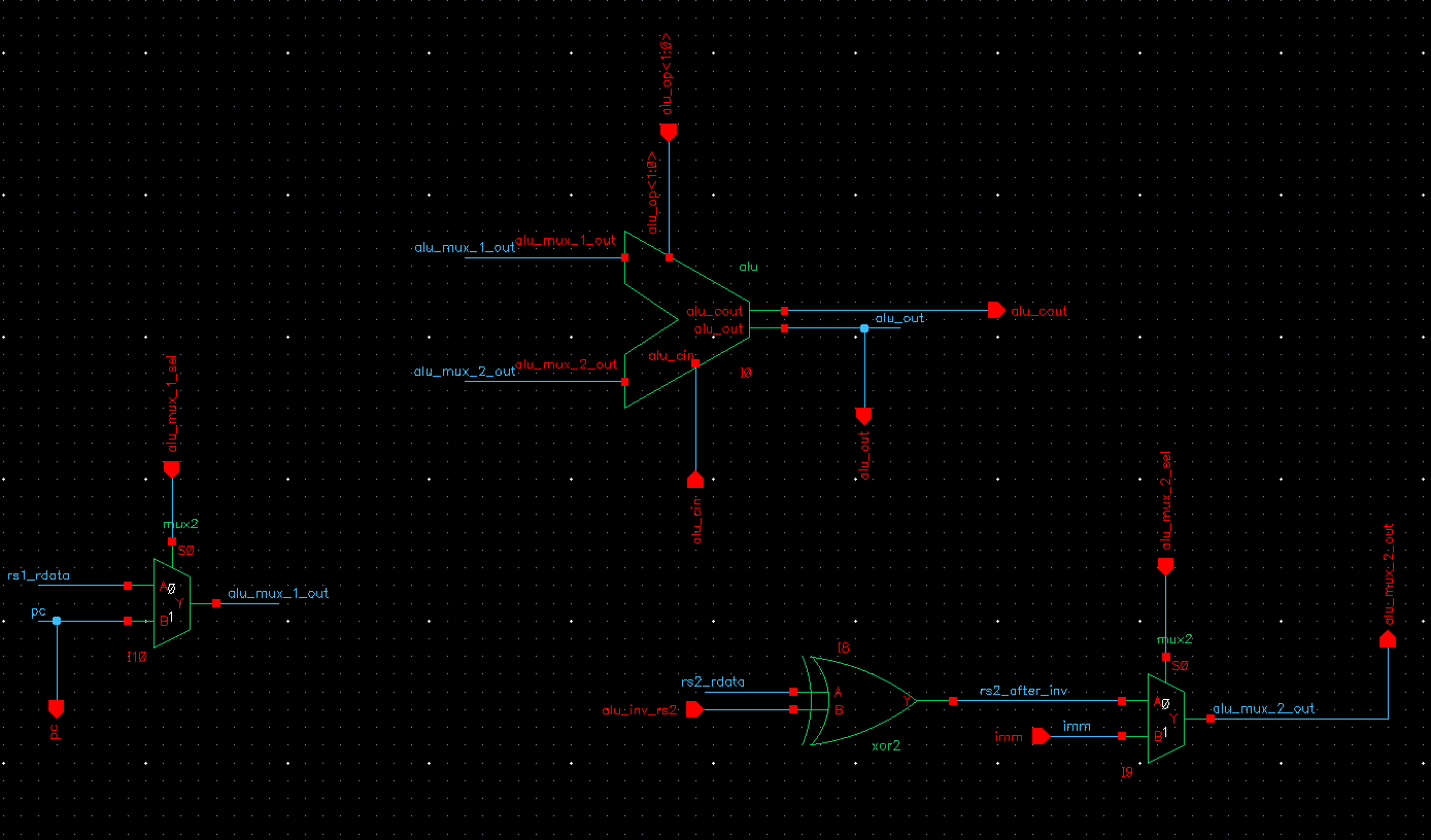
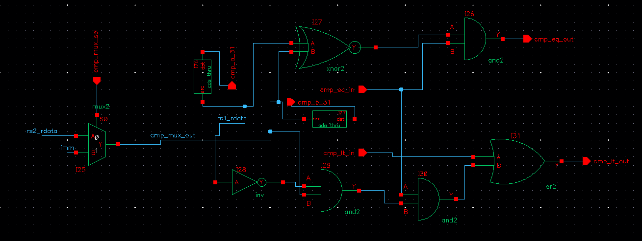
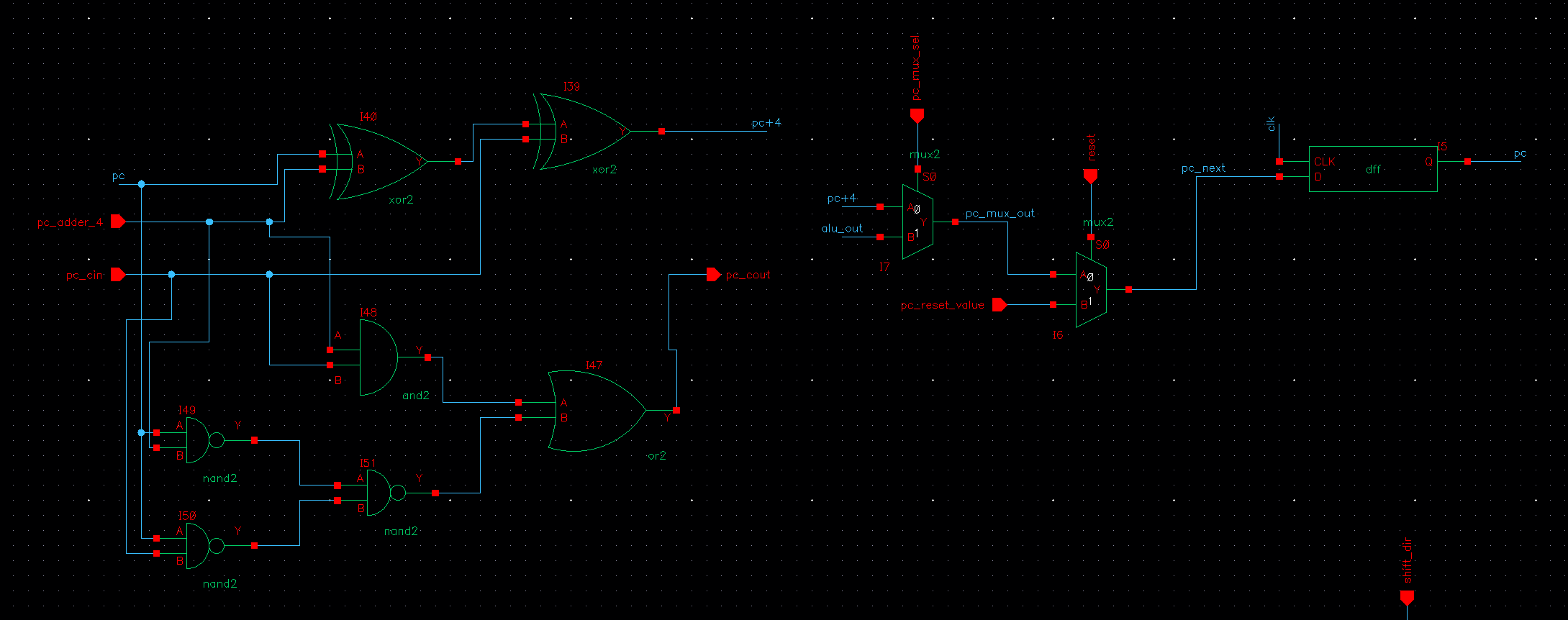
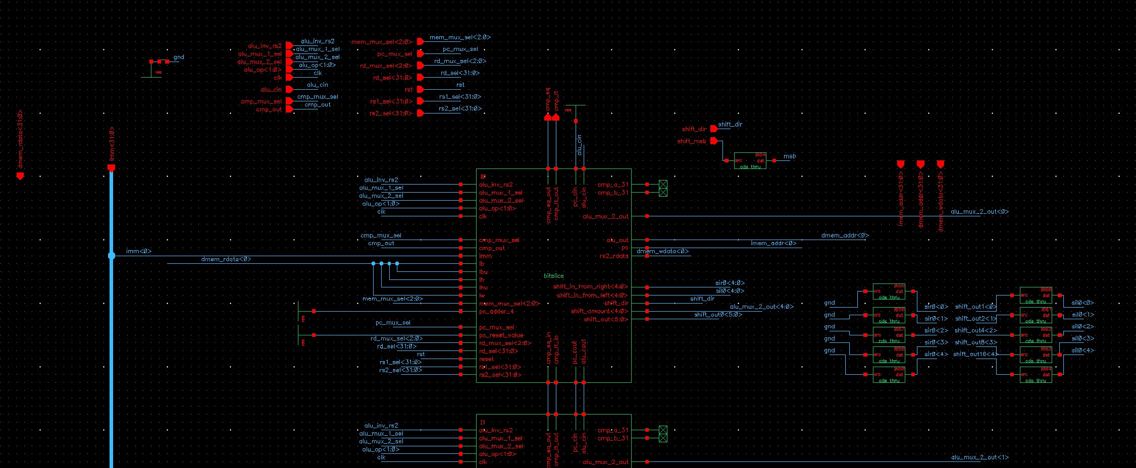
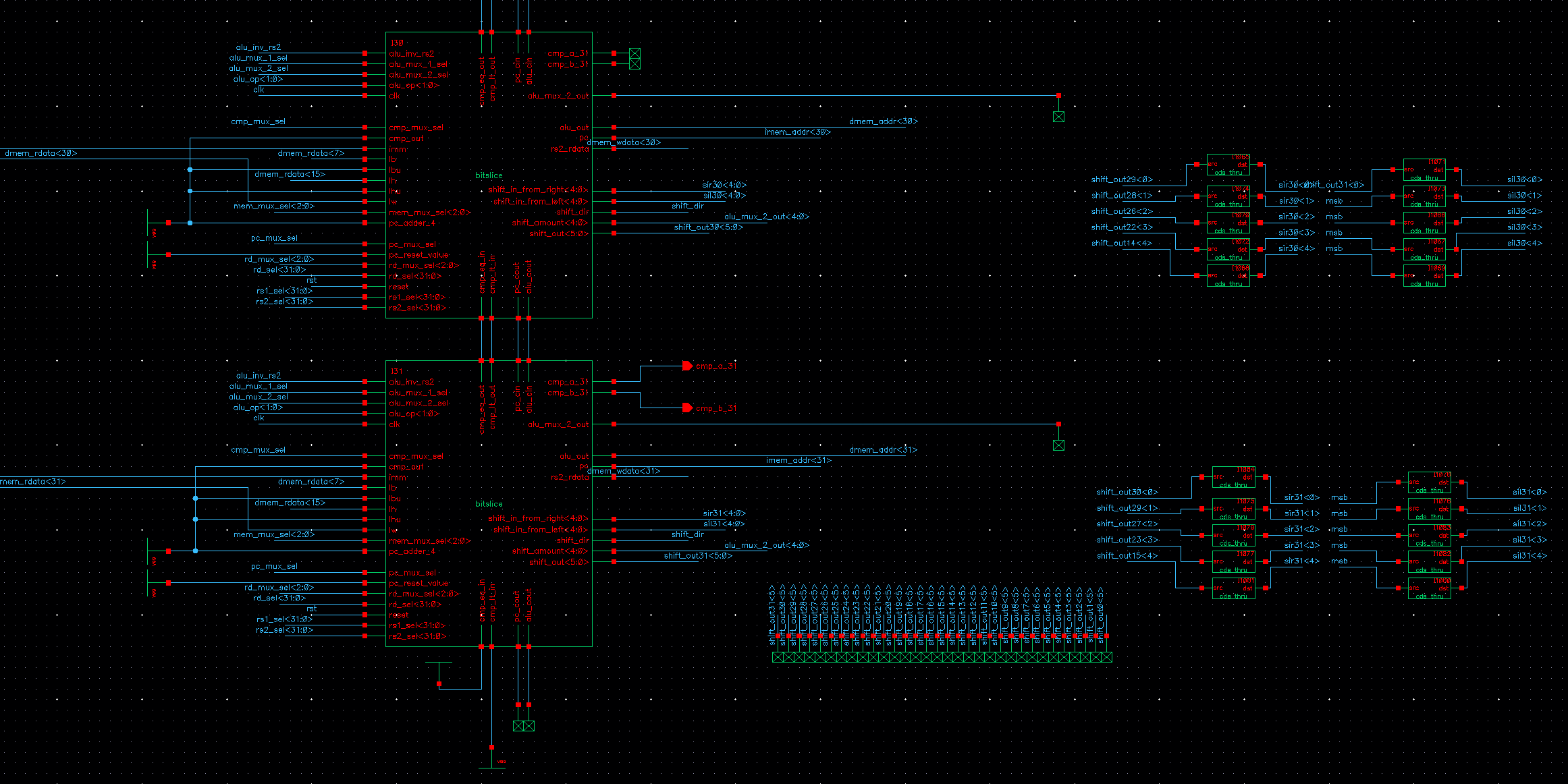
The ALU supports addition, subtraction, bitwise AND/OR/XOR, and comparison operations. It is constructed hierarchically from the standard cell library and laid out column-by-column within the bitslice. Carry propagation is handled at the bitslice boundary.
The fundamental storage primitive built from the DFF cell. Stores one bit of architectural state and is tiled to form registers across the full 32-bit width.
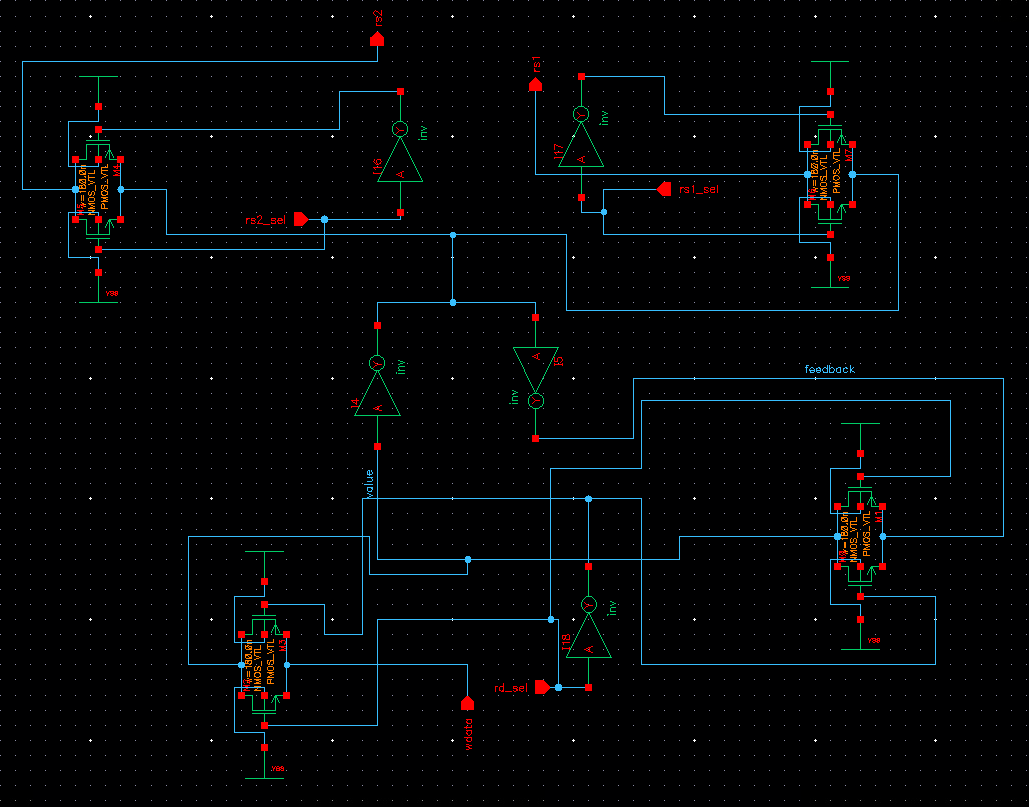
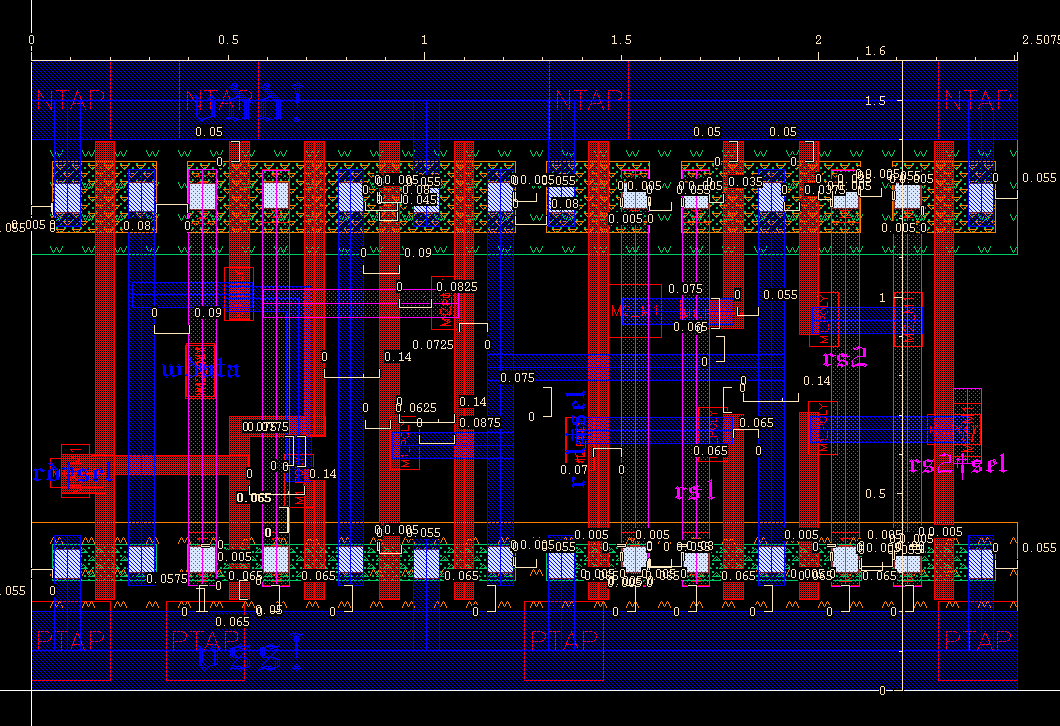
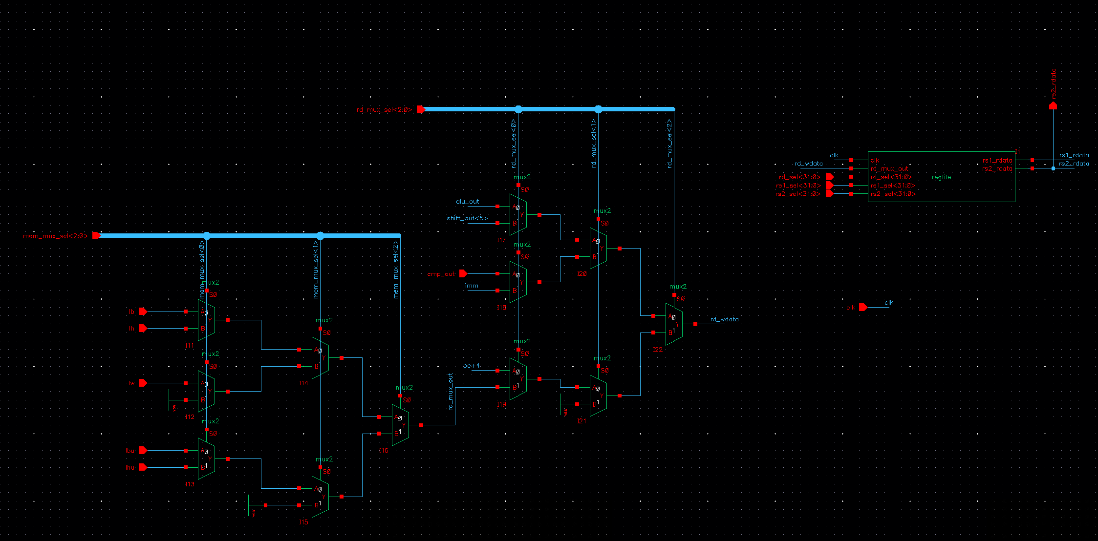
A 32×32 register file providing two read ports and one write port. The array of 1-bit registers is organized in a bitslice column layout, with shared wordline and bitline routing at the cell boundary.
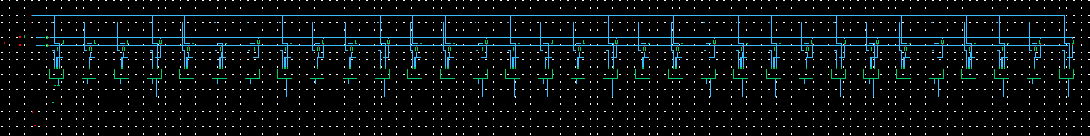
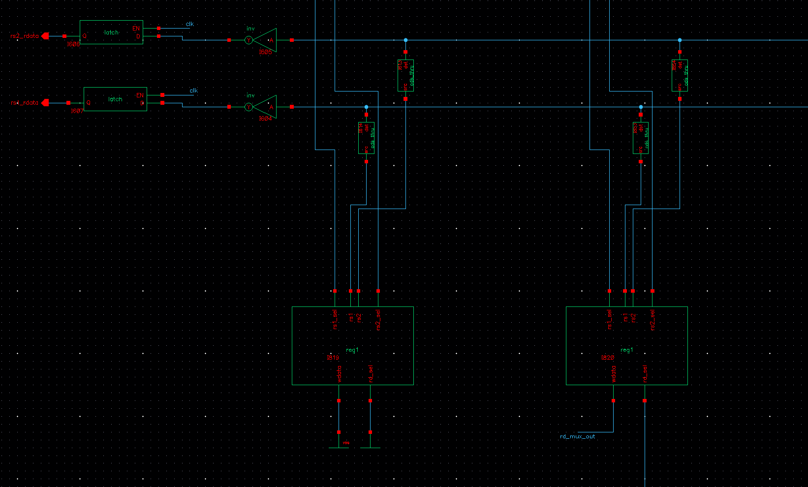
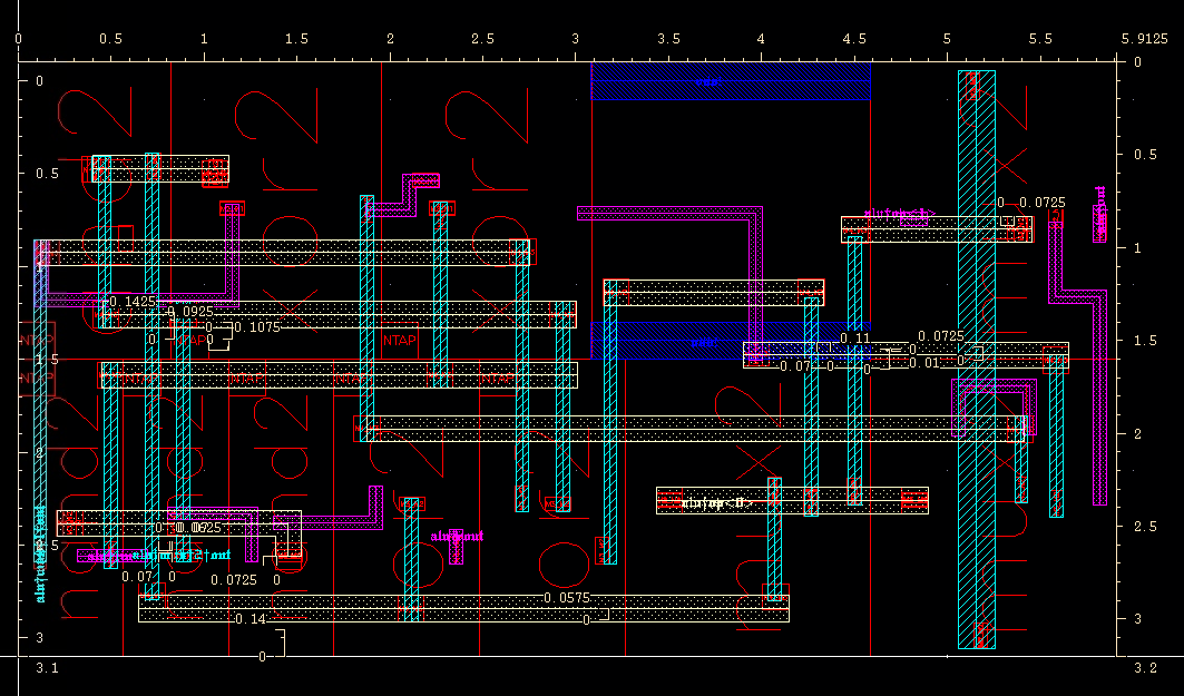
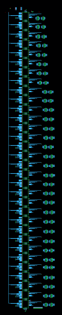
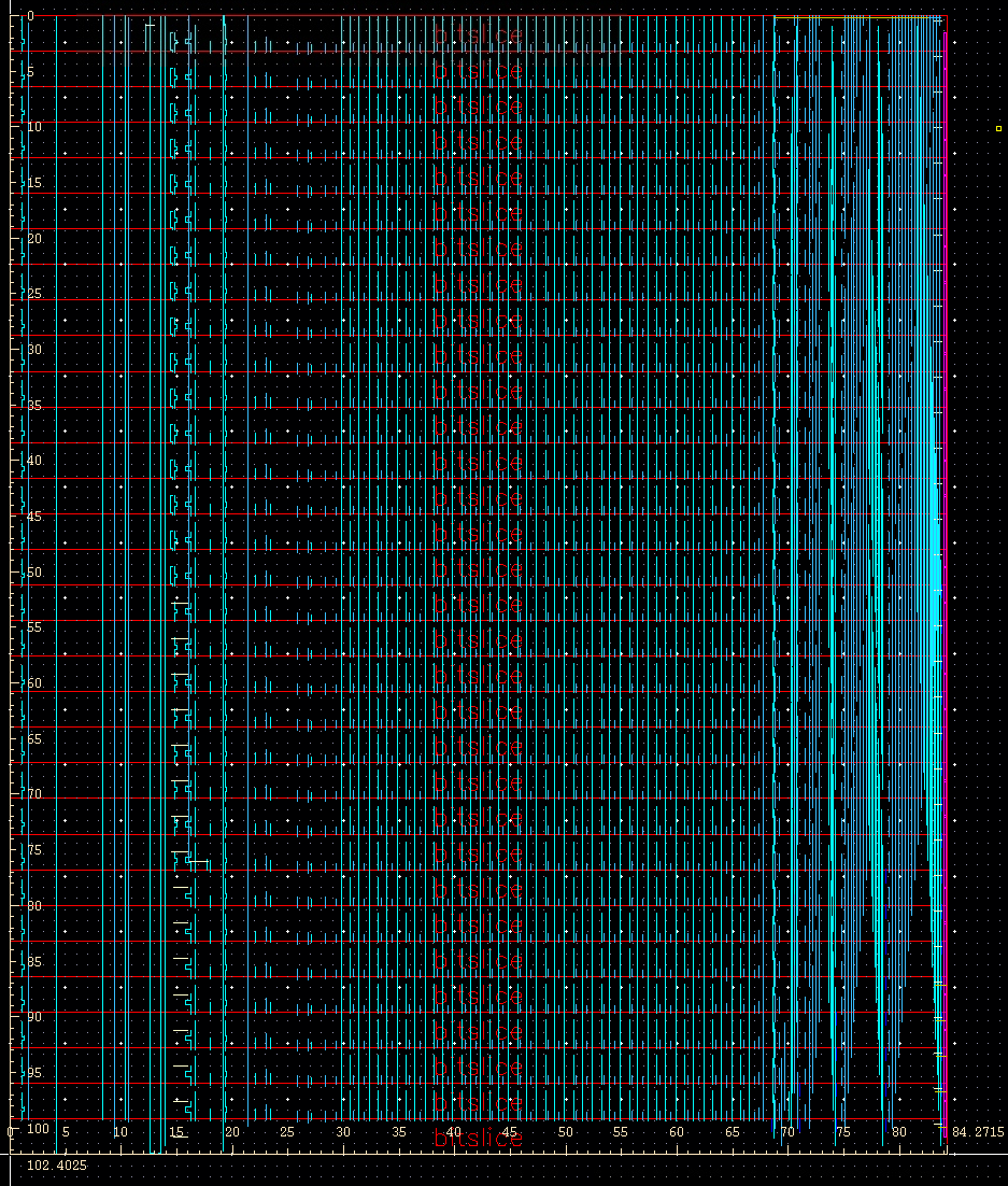
One complete bitslice column encapsulating ALU, barrel shifter, comparator, PC register, and register file write logic. Tiling 32 of these columns produces the complete datapath. The componized layout view breaks the design into labeled functional blocks.

The complete 32-bit datapath assembled from 32 bitslice columns. Top and bottom schematic views capture the full signal routing, and the DRC/LVS results confirm a clean design at the top level.
Control Unit Integration
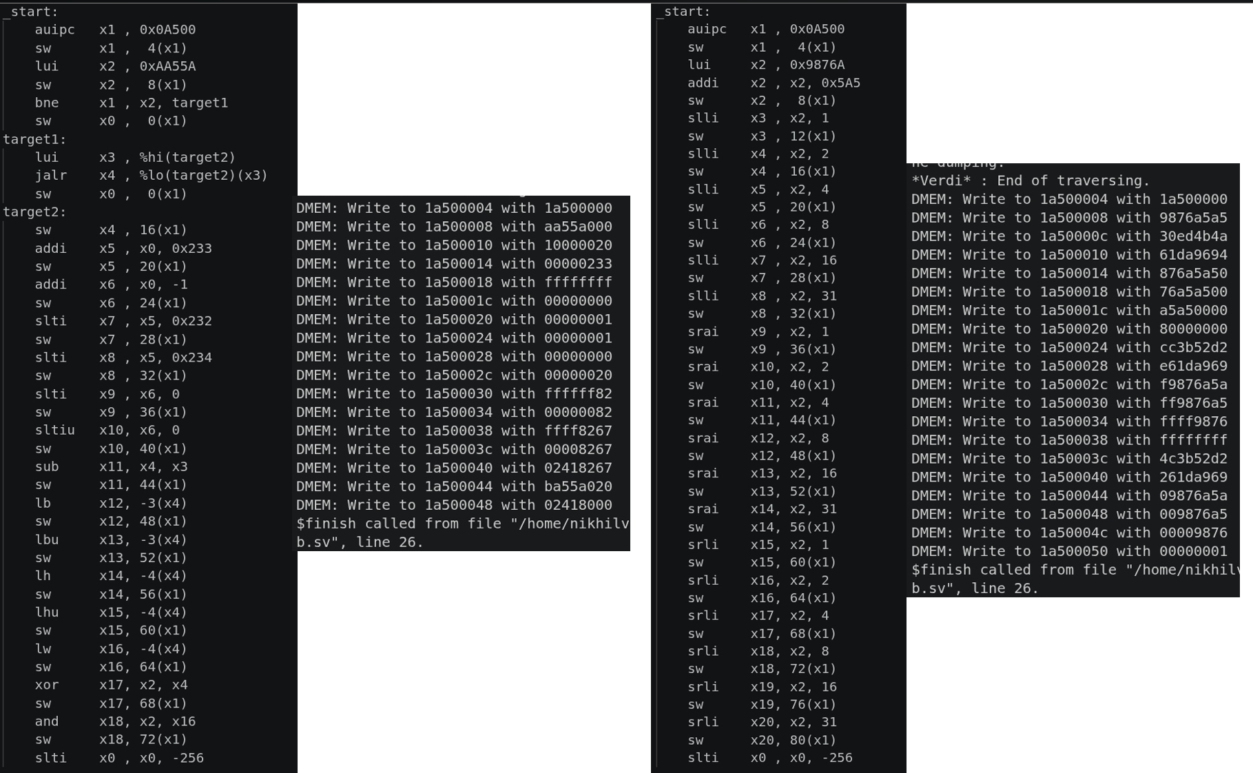
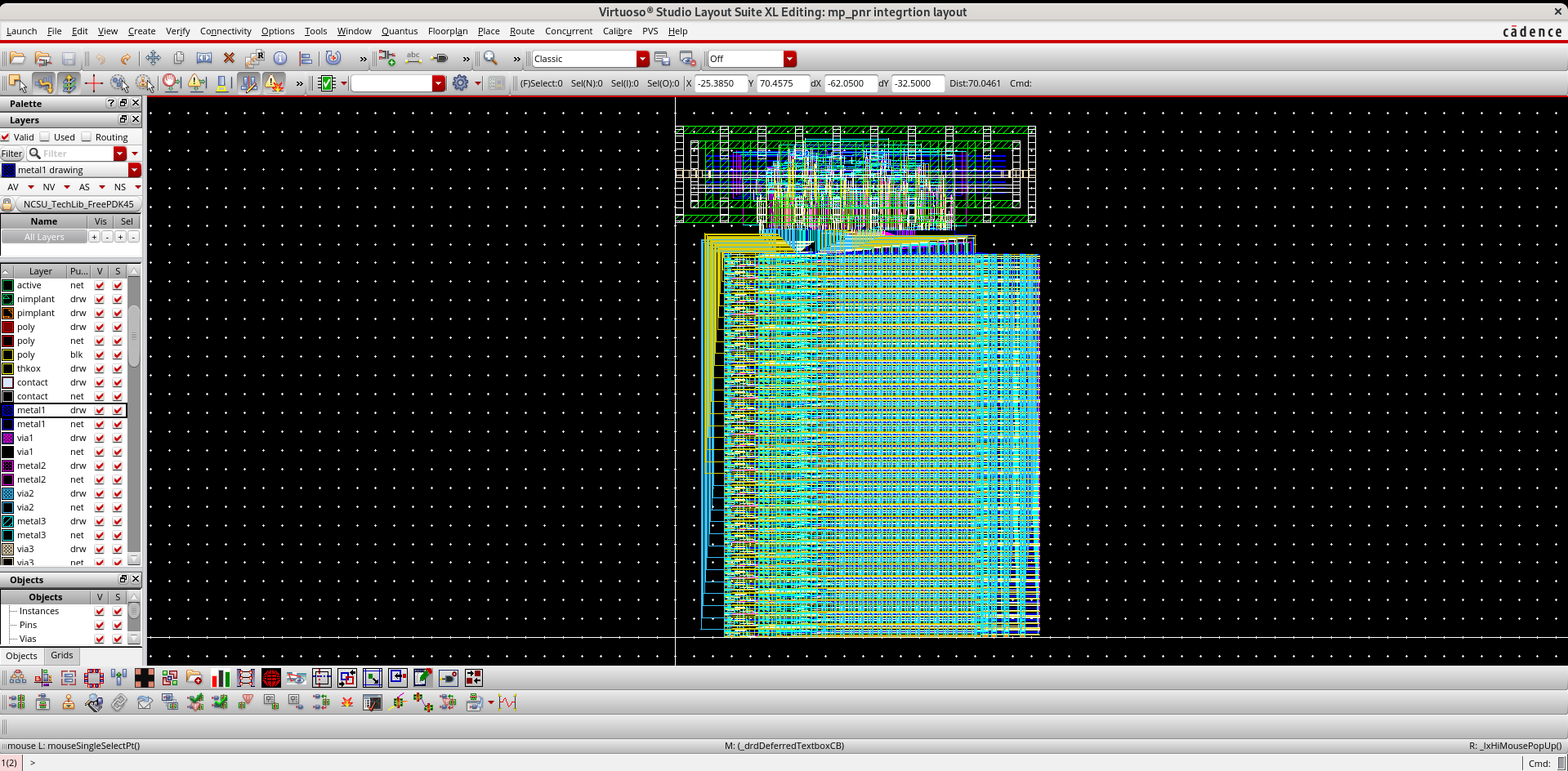
With the full-custom datapath complete, a RISC-V control unit was written in RTL, synthesized using Synopsys Design Compiler against the custom standard cell library, and placed-and-routed with Cadence Innovus. The resulting GDSII was then imported back into Cadence Virtuoso and manually connected to the hand-crafted datapath, producing a complete CPU layout.
Two full-chip configurations were produced: one using the synthesized standard cells throughout, and one retaining the hand-built register file from the datapath. Both were verified for layout connectivity.
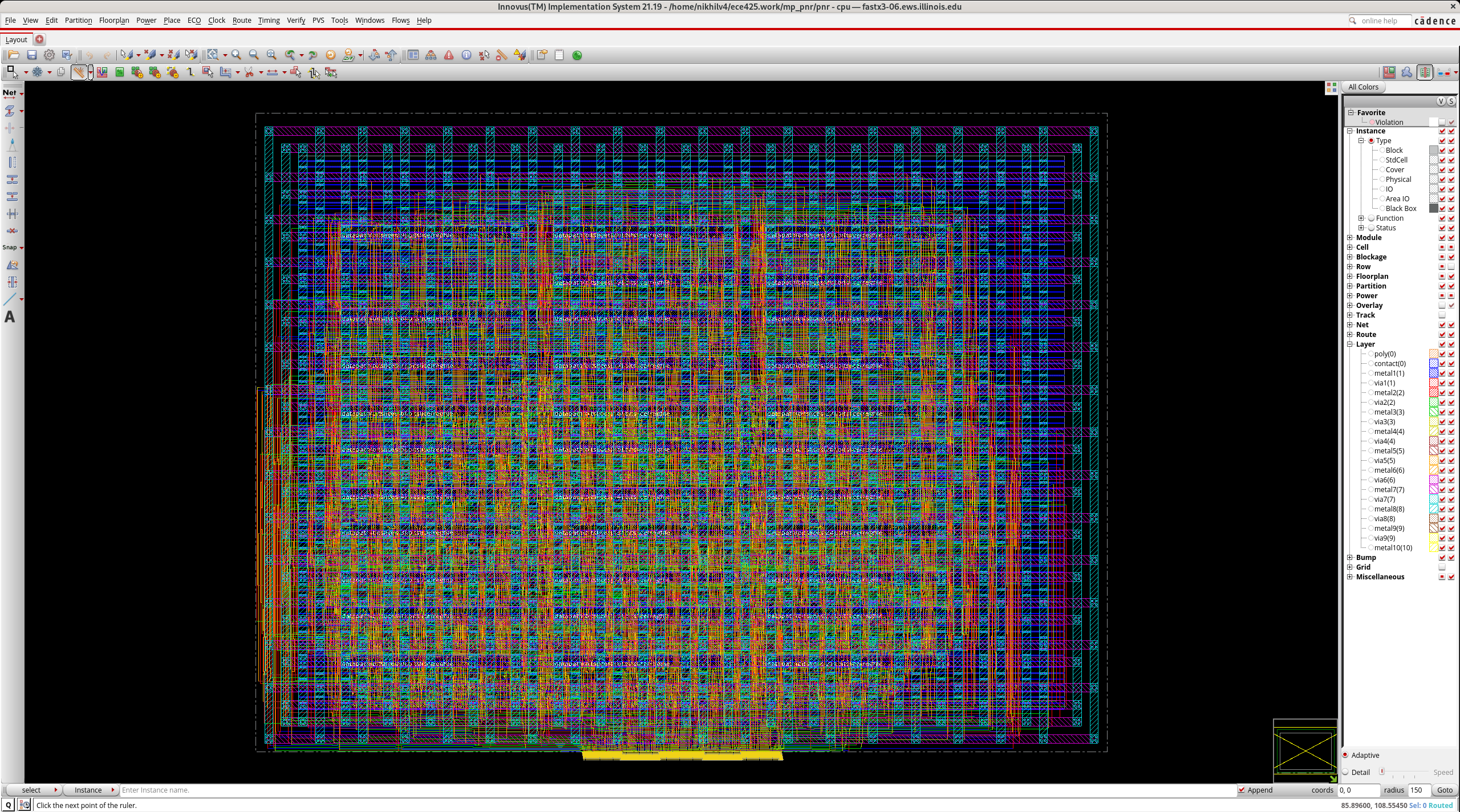
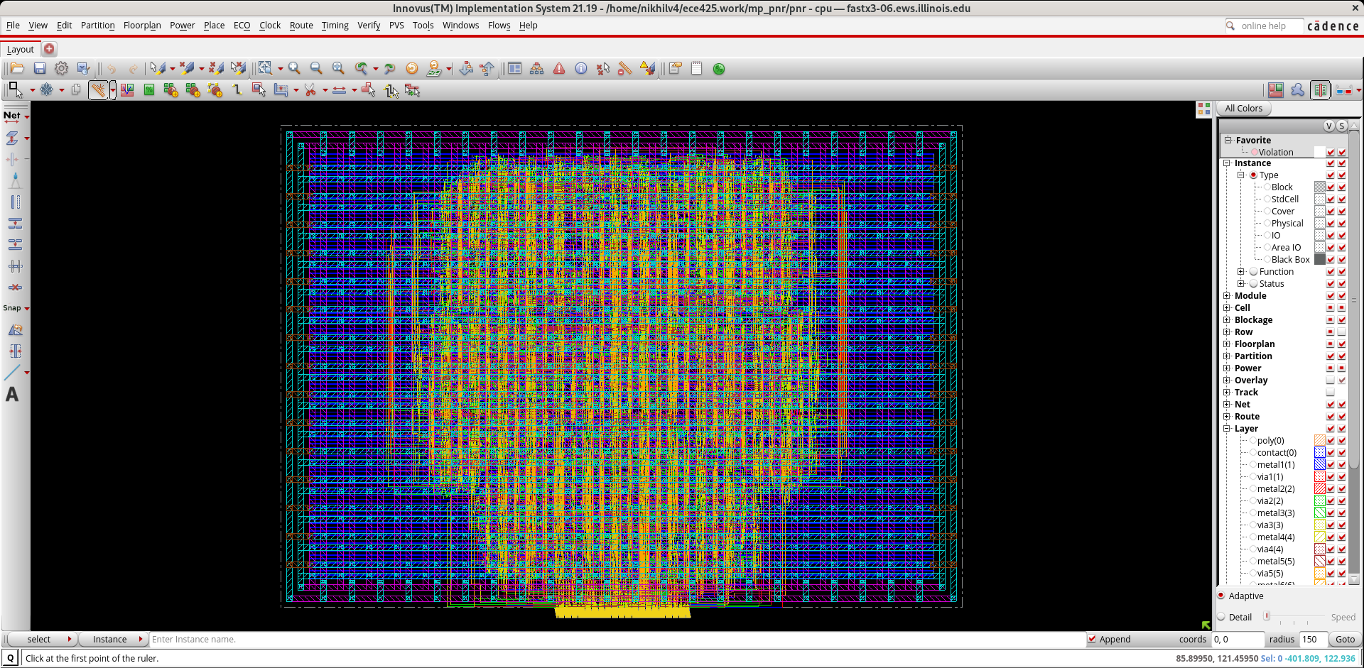
The RISC-V control unit RTL was synthesized and placed-and-routed using Cadence Innovus with the custom standard cell library as the target technology. The resulting layout encodes all instruction decode, control signal generation, and branch resolution logic.
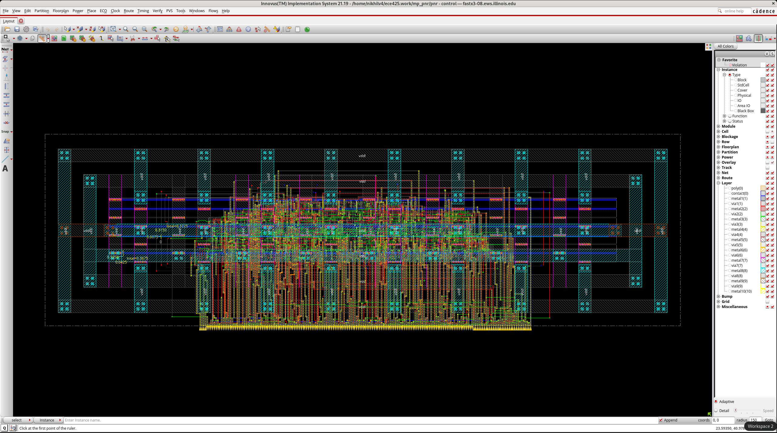
The Innovus-generated control unit was imported into Cadence Virtuoso and manually wired to the custom datapath. Metal routing bridges the synthesized block and the hand-crafted bitsliced datapath, completing the full processor.
Complete CPU layout with the control unit and a datapath built entirely from the synthesized standard cell library. All logic — datapath and control — is instantiated from the same cell set, giving a unified, consistent floorplan.
Alternate full-chip configuration that retains the hand-crafted register file from the original datapath alongside the Innovus-synthesized control unit. The custom register file occupies a clearly visible block, illustrating the hybrid full-custom / automated design flow.